Whenever the topic nano technology comes up most of us don’t have a clear idea of what it is. Especially when it is about the difference between nano science and nano technology. Then what is nano science?
Nanoscience is the study of objects with size less than hundred nanometers at least in one dimension. When objects go to nanometer scale in size, their behavior get changed applied laws may not be the same as when they were larger in size. Nanoscience involves finding governing laws of these tiny objects, deriving theoretical models to describe the behavior of those nanoscale materials and analyzing the properties of them.
So, what is Nano technology?
Nanotechnology is engineering the nanoscale objects at molecular level using different techniques. Nanotechnology is all about techniques and tools to come up with a nanoscale design or system that exploit the properties at molecular level to be more accurate and efficient.
Using the knowledge on material behaviour at nanoscale which is got from nanoscience, nanotechnology focuses on properties such as strength, lightness, electrical and thermal conductance and reactivity to design and manufacture useful items.
How did all start?
The emergence of nanotechnology in the 1980s was caused by the convergence of experimental advances such as the invention of the scanning tunneling microscope in 1981 and the discovery of fullerenes in 1985, with the elucidation and popularization of a conceptual framework for the goals of nanotechnology beginning with the 1986 publication of the book Engines of Creation.
The conceptual origin
The American physicist Richard Feynman lectured, “There’s Plenty of Room at the Bottom,” at an American Physical Society meeting at Caltech on December 29, 1959, which is often held to have provided inspiration for the field of nanotechnology. Feynman had described a process by which the ability to manipulate individual atoms and molecules might be developed, using one set of precise tools to build and operate another proportionally smaller set, so on down to the needed scale. In the course of this, he noted, scaling issues would arise from the changing magnitude of various physical phenomena: gravity would become less important, surface tension and Van der Waals attraction would become more important.
The Japanese scientist called Norio Taniguchi of Tokyo University of Science was the first to use the term “nano-technology” in a 1974 conference,[11] to describe semiconductor processes such as thin film deposition and ion beam milling exhibiting characteristic control on the order of a nanometer. His definition was, “‘Nano-technology’ mainly consists of the processing of, separation, consolidation, and deformation of materials by one atom or one molecule.” However, the term was not used again until 1981 when Eric Drexler, who was unaware of Taniguchi’s prior use of the term, published his first paper on nanotechnology in 1981.
In the 1980s the idea of nanotechnology as a deterministic, rather than stochastic, handling of individual atoms and molecules was conceptually explored in depth by K. Eric Drexler, who promoted the technological significance of nano-scale phenomena and devices through speeches and two influential books.
In 1980, Drexler encountered Feynman’s provocative 1959 talk “There’s Plenty of Room at the Bottom” while preparing his initial scientific paper on the subject, “Molecular Engineering: An approach to the development of general capabilities for molecular manipulation,” published in the Proceedings of the National Academy of Sciences in 1981.[1] The term “nanotechnology” (which paralleled Taniguchi’s “nano-technology”) was independently applied by Drexler in his 1986 book Engines of Creation: The Coming Era of Nanotechnology, which proposed the idea of a nanoscale “assembler” which would be able to build a copy of itself and of other items of arbitrary complexity. He also first published the term “grey goo” to describe what might happen if a hypothetical self-replicating machine, capable of independent operation, were constructed and released.
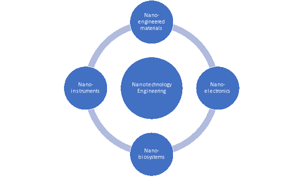 Nanotechnology is a multi-disciplinary engineering field, which draws from and benefits areas such as materials science and engineering, chemistry, physics, biology, and medicine
Nano-engineered materials, addresses the synthesis, characterization and engineering application of several classes of advanced materials, including nanocrystalline materials and nanopowders used in electronics and photonics applications, as catalysts in automobiles, in the food and pharmaceutical industries, as membranes for fuel cells, and for industrial-scale polymers.
Nano-electronics, addresses the development of systems and materials that will enable the electronics industry to overcome current technological limits. Also part of this theme area is a new generation of electronics based on plastics, which is expected to create new markets with applications ranging from smart cards to tube-like computers.
Nano-biosystems, addresses the molecular manipulation of biomaterials and the engineering of nanoscale systems and processes of biological and medicinal interest, such as, for example, the targeted delivery of therapeutic agents and the design of DNA, peptide, protein, and cell chips.
Nano-instruments addresses some of the most far-reaching yet practical applications of miniature instruments for measuring atoms or molecules in chemical, clinical, or biochemical analysis; in biotechnology for agent detection; and environmental analysis.
 What do we have so far?
 scientists at the Department of Energy’s Oak Ridge National Laboratory have developed a catalyst made of carbon, copper and nitrogen and applied voltage to trigger a complicated chemical reaction that essentially reverses the combustion process. With the help of the nanotechnology-based catalyst which contains multiple reaction sites, the solution of carbon dioxide dissolved in water turned into ethanol with a yield of 63 percent. Typically, this type of electrochemical reaction results in a mix of several different products in small amounts.
The ideas and concepts behind nanoscience and nanotechnology started with a talk entitled “There’s Plenty of Room at the Bottom” by physicist Richard Feynman at an American Physical Society meeting at the California Institute of Technology (CalTech) on December 29, 1959, long before the term nanotechnology was used. In his talk, Feynman described a process in which scientists would be able to manipulate and control individual atoms and molecules. Over a decade later, in his explorations of ultraprecision machining, Professor Norio Taniguchi coined the term nanotechnology. It wasn’t until 1981, with the development of the scanning tunneling microscope that could “see” individual atoms, that modern nanotechnology began.
 Manufacturing at the nanoscale is known as nanomanufacturing. Nanomanufacturing involves scaled-up, reliable, and cost-effective manufacturing of nanoscale materials, structures, devices, and systems. It also includes research, development, and integration of top-down processes and increasingly complex bottom-up or self-assembly processes.

A product of nanomanufacturing: A 16 gauge wire (above), approximately 1.3 millimeters in diameter, made from carbon nanotubes that were spun into thread. And the same wire on a 150 ply spool (below.) Courtesy of Nanocomp.
In more simple terms, nanomanufacturing leads to the production of improved materials and new products. As mentioned above, there are two basic approaches to nanomanufacturing, either top-down or bottom-up. Top-down fabrication reduces large pieces of materials all the way down to the nanoscale, like someone carving a model airplane out of a block of wood. This approach requires larger amounts of materials and can lead to waste if excess material is discarded. The bottom-up approach to nanomanufacturing creates products by building them up from atomic- and molecular-scale components, which can be time-consuming. Scientists are exploring the concept of placing certain molecular-scale components together that will spontaneously “self-assemble,” from the bottom up into ordered structures.
Within the top-down and bottom-up categories of nanomanufacturing, there are a growing number of new processes that enable nanomanufacturing. Among these are:
Structures and properties of materials can be improved through these nanomanufacturing processes. Such nanomaterials can be stronger, lighter, more durable, water-repellent, anti-reflective, self-cleaning, ultraviolet- or infrared-resistant, antifog, antimicrobial, scratch-resistant, or electrically conductive, among other traits. Taking advantage of these properties, today’s nanotechnology-enabled products range from baseball bats and tennis rackets to catalysts for refining crude oil and ultrasensitive detection and identification of biological and chemical toxins.
|
|
|
A high resolution image of a graphene transistor with a sheet of carbon only one atom thick. This high speed electronic device was created using nanoscale processes, and may one day be used for better computer hips. (Courtesy of James Yardley, Columbia University Nanocenter, an NNI-sponsored NSEC) |
Nanoscale transistors may someday lead to computers that are faster, more powerful, and more energy efficient than those used today. Nanotechnology also holds the potential to exponentially increase information storage capacity; soon your computer’s entire memory will be able to be stored on a single tiny chip. In the energy arena, nanotechnology will enable high-efficiency, low-cost batteries and solar cells.
For more products and applications that use nanotechnology, see Benefits & Applications or browse our database of the NNI’s Major Achievements in Nanotechnology.
Nanotechnology R&D, and the eventual nanomanufacturing of products, requires advanced and often very expensive equipment and facilities. In order to realize the potential of nanotechnology, NNI agencies are investing heavily in nanomanufacturing R&D and infrastructure. Over 90 NNI-funded centers and user facilities across the country provide researchers the facilities, equipment, and trained staff to develop nanotechnology applications and associated manufacturing processes.
The NNI helps drive the nanomanufacturing field by providing researchers and small businesses with access to this specialized equipment in order to maintain global U.S. competitiveness. To assist in agency coordination in the area of nanomanufacturing, the Nanoscale Science, Engineering, and Technology (NSET) Subcommittee created the Nanotechnology Innovation and Commercialization Ecosystem (NICE) Working Group.
The President’s FY 2017 Budget provides $1.4 billion for the National Nanotechnology Initiative, including an estimated $37 million for nanomanufacturing.
The National Nanomanufacturing Network (NNN) is an alliance of academic, government and industry partners that cooperate to advance nanomanufacturing strength in the U.S. The NNI and its member agencies actively participate in, support, and contribute to the NNN in its mission to advance nanomanufacturing.
The NNN functions as part electronic resource, part community of practice, and part network of experts working on the development of nanomanufacturing. The NNN fosters technology transition and exchange through a host of activities including reviews and archiving of emerging materials, processes, and areas of practice, strategic workshops and roadmap development. InterNano is the information arm of the NNN-a digital library resource of timely information on nanomanufacturing and a platform for collaboration, providing information archiving in areas of processes and tools, standards, reports, events, and environmental health and safety databases.

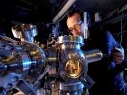 A scanning tunneling microscope (STM) is an instrument for imaging surfaces at the atomic level. Its development in 1981 earned its inventors, Gerd Binnig and Heinrich Rohrer (at IBM Zürich), the Nobel Prize in Physics in 1986.[1][2] For a STM, good resolution is considered to be 0.1 nm lateral resolution and 0.01 nm (10 pm) depth resolution.[3] With this resolution, individual atoms within materials are routinely imaged and manipulated. The STM can be used not only in ultra-high vacuum but also in air, water, and various other liquid or gas ambients, and at temperatures ranging from near zero kelvin to over 1000°C.[4][5]
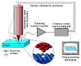 STM is based on the concept of quantum tunneling. When a conducting tip is brought very near to the surface to be examined, a bias (voltage difference) applied between the two can allow electrons to tunnel through the vacuum between them. The resulting tunneling current is a function of tip position, applied voltage, and the local density of states (LDOS) of the sample.[4]Information is acquired by monitoring the current as the tip’s position scans across the surface, and is usually displayed in image form. STM can be a challenging technique, as it requires extremely clean and stable surfaces, sharp tips, excellent vibration control, and sophisticated electronics, but nonetheless many hobbyists have built their own.
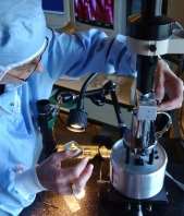 Atomic-force microscopy (AFM) or scanning-force microscopy (SFM) is a type of scanning probe microscopy (SPM), with demonstrated resolution on the order of fractions of a nanometer, more than 1000 times better than the optical diffraction limit. The information is gathered by “feeling” or “touching” the surface with a mechanical probe. Piezoelectric elements that facilitate tiny but accurate and precise movements on (electronic) command enable very precise scanning.
The AFM has three major abilities: force measurement, imaging, and manipulation.
You have to be 100% sure of the quality of your product to give a money-back guarantee. This describes us perfectly. Make sure that this guarantee is totally transparent.
Read moreEach paper is composed from scratch, according to your instructions. It is then checked by our plagiarism-detection software. There is no gap where plagiarism could squeeze in.
Read moreThanks to our free revisions, there is no way for you to be unsatisfied. We will work on your paper until you are completely happy with the result.
Read moreYour email is safe, as we store it according to international data protection rules. Your bank details are secure, as we use only reliable payment systems.
Read moreBy sending us your money, you buy the service we provide. Check out our terms and conditions if you prefer business talks to be laid out in official language.
Read more